Hi,welcome To Login SZ HONGXIN MICRO TECH CO., LTD-----SZ HONGXIN MICRO TECH CO., LTD!
- Login Register Collection
- |
- |

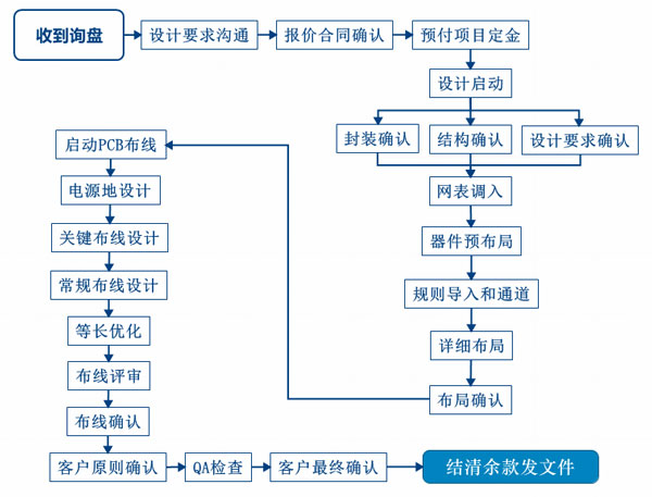
PCB design service process
SZ HONGXIN MICRO TECH CO., LTD CAD design business for many yearsMainly undertake Multi-layer, high-density PCB design panel Business.Have PCB design team with an average of more than five years of work experience,able Proficiency in the market mainstream PCB design software, Professional high-efficiency communication guarantees PCB design progress to help you seize market opportunities earlier!
PCB design business areas:
Communication product board design | GSM/GPRS,switch,RFEquipment, etc. |
Numbers/Digital product board design | Set top box, HD TV, digital camera, camera, etc. |
Security product board design | Video monitoring, intercom |
PCAnd related product board design | MB、NB、SERVERMotherboard and various types of industrial control boards, etc. |
PCB Design Our Common Software:
Allegro, Pads, Protel, Orcad, AD, Pads_Logic, etc.;PS: We can convert the ORCAD format conversion according to the PDF schematic provided by customers, and then import menu.
PCB design regular delivery:
In the schematic determination, the device package is completely on the design cycle as follows:
Layer number | Design cycle |
2Laminate | 2-3Working day |
4Laminate | 4-5Working day |
6Laminate | 6-7Working day |
8Laminate | 7-8Working day |
10Laminate | 10-12Working day |
PS: The above is delivered for regular delivery, accurately design delivery, according to the number of pieces of the circuit board, the extent, the level, and other factors!